


- Obecnie brak na stanie


ARM7TDMI, 512kB Flash (ISP), 64kB RAM, 2xCAN, Ethernet 10/100, USB, DMA, I2S, 3xI2C, SPI/SSP, 4xUART, ADC, DAC, LQFP100, RoHS

darmowa wysyłka na terenie Polski dla wszystkich zamówień powyżej 500 PLN

Jeśli Twoja wpłata zostanie zaksięgowana na naszym koncie do godz. 11:00

Każdy konsument może zwrócić zakupiony towar w ciągu 14 dni bez zbędnych pytań
LPC2387FBD100
ARM7TDMI, 512kB Flash (ISP), 64kB RAM, 2xCAN, Ethernet 10/100, USB, DMA, I2S, 3xI2C, SPI/SSP, 4xUART, ADC, DAC, LQFP100, RoHS.
Download:
Cechy
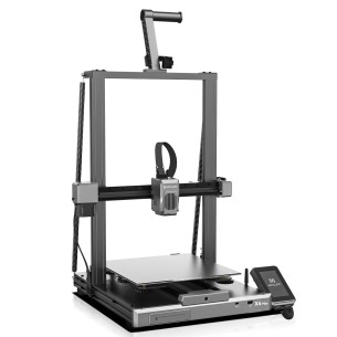
Brak towaru
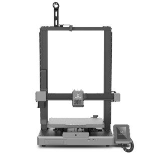
Brak towaru
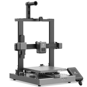
Brak towaru
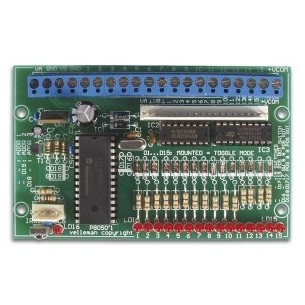
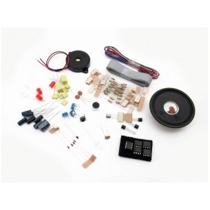
15 kanałowy odbiornik podczerwieni - zestaw do samodzielnego montażu
Brak towaru
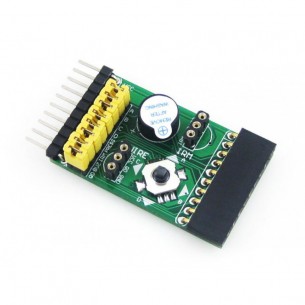
Waveshare Mix Board, płytka przejściowa 4 w 1, zawiera czujnik temperatury, odbiornik podczerwieni, joystick i buzzer
Brak towaru
Brak towaru
Brak towaru
Brak towaru
Zmontowany uniwersalny komputer samochodowy, przeznaczony dla osób, które chcą podwyższyć funkcjonalność swojego samochodu. AVT5495 C
Brak towaru
EMULATOR-PROGRAMATOR MIKROKONTROLERÓW AVR I `51 - PŁYTKA DRUKOWANA I ZAPROGRAMOWANY UKŁAD
Brak towaru
Brak towaru
Brak towaru
Nakrętka sześciokątna ocynk M2,5, wysokość 2mm, DIN934, RoHS
Brak towaru
Brak towaru
Brak towaru
Brak towaru
ARM7TDMI, 512kB Flash (ISP), 64kB RAM, 2xCAN, Ethernet 10/100, USB, DMA, I2S, 3xI2C, SPI/SSP, 4xUART, ADC, DAC, LQFP100, RoHS