


101,76 zł Netto
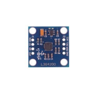
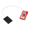
L3G4200D 3-Axis Gyro Carrier with Voltage Regulator umożliwia dokładny pomiar prędkości kątowej w trzech osiach przy prostej integracji z systemami sterowania. Moduł sprawdza się w projektach wymagających stabilizacji, kontroli orientacji oraz analizy ruchu w robotyce i mechatronice. Pololu 1272
Pololu 1272 – L3G4200D 3-Axis Gyro Carrier with Voltage Regulator przeznaczony do pomiaru prędkości kątowej wokół trzech osi w projektach robotycznych, mechatronicznych i systemach nawigacyjnych. Moduł oparty na czujniku MEMS L3G4200D umożliwia precyzyjny pomiar obrotu w osiach X, Y i Z, co pozwala na realizację funkcji stabilizacji, detekcji ruchu oraz estymacji orientacji przestrzennej.
Zintegrowany stabilizator napięcia umożliwia zasilanie modułu z szerszego zakresu napięć, co upraszcza integrację z mikrokontrolerami pracującymi zarówno z logiką 3,3 V, jak i 5 V. Komunikacja odbywa się poprzez interfejs cyfrowy I²C lub SPI, zapewniając wysoką odporność na zakłócenia i łatwe połączenie z popularnymi platformami rozwojowymi. Moduł znajduje zastosowanie w robotach mobilnych, systemach balansujących, platformach pomiarowych oraz projektach edukacyjnych.
Producent BTC Korporacja sp. z o. o. Lwowska 5 05-120 Legionowo Polska sprzedaz@kamami.pl 22 767 36 20
Osoba odpowiedzialna BTC Korporacja sp. z o. o. Lwowska 5 05-120 Legionowo Polska sprzedaz@kamami.pl 22 767 36 20
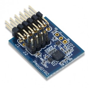
PmodGYRO, moduł z 3-osiowym żyroskopem L3G4200D, SPI, I2C, 800 Hz. Digilent 410-215
Brak towaru
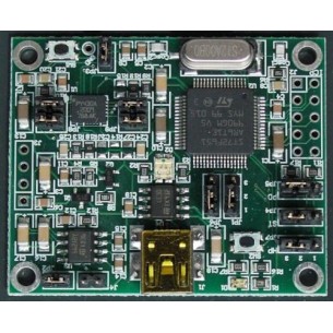
Płytka STEVAL-MKI079V1 umożliwia prezentację i testowanie działania dwukanałowego żyroskopu LPR430AL w trybie analogowym lub cyfrowym. Wbudowany mikrokontroler i interfejs USB ułatwiają analizę sygnałów oraz rozwój aplikacji opartych na czujnikach MEMS w systemach pomiarowych i sterujących.
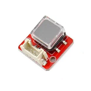
Moduł z układem L3G4200D (3-osiowy żyroskop z wyjściem cyfrowym)
L3G4200D 3-Axis Gyro Carrier with Voltage Regulator umożliwia dokładny pomiar prędkości kątowej w trzech osiach przy prostej integracji z systemami sterowania. Moduł sprawdza się w projektach wymagających stabilizacji, kontroli orientacji oraz analizy ruchu w robotyce i mechatronice. Pololu 1272
Moduł 3-osiowego żyroskopu z układem L3G4200D, wyposażony w interfejsy I2C i SPI. Zasilanie napięciem 3..5 V, w komplecie złącza 2,54 mm proste i kątowe. GY-50
Brak towaru
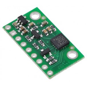
Prosty w użyciu moduł z 3-osiowym żyroskopem L3GD20, interfejs I2C lub SPI, zasilanie 2.5..5.5V, regulator napięcia wyjściowego 3.3V, regulowany szerszy zakres czułości ±245°/s, ±500°/s, lub ±2000°/s, kompatybilny z Arduino i Raspberry Pi. Pololu 2129
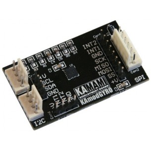
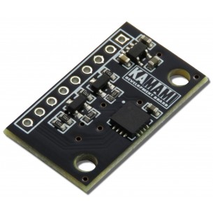
KAmodL3GD20 to moduł żyroskopu cyfrowego z układem L3GD20. Pozwala na pomiar prędkości kątowej do ±2000 stopni na sekundę. KAmodL3GD20
Crowtail – 3-Axis Digital Gyro to moduł żyroskopowy z układem ITG-3200 oferujący pomiar ruchu obrotowego w trzech osiach z dużą precyzją. Przeznaczony do projektów interaktywnych, robotyki, systemów sterowania i urządzeń reagujących na ruch.
L3G4200D 3-Axis Gyro Carrier with Voltage Regulator umożliwia dokładny pomiar prędkości kątowej w trzech osiach przy prostej integracji z systemami sterowania. Moduł sprawdza się w projektach wymagających stabilizacji, kontroli orientacji oraz analizy ruchu w robotyce i mechatronice. Pololu 1272