


- Out-of-Stock


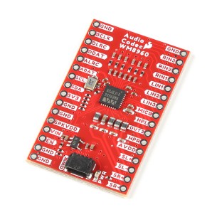
WM8960 stereo codec module with driver for 1W class D speakers and headphones. It uses the I2S interface and the I2C bus to configure the system. SparkFun BOB-21250
No product available!
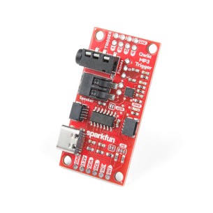
MP3 player module controlled by I2C interface or switching inputs. It is based on a 1.4 W audio amplifier. The board has a 3.5 mm audio output and a connector for connecting a loudspeaker. Files are played from a microSD card. SparkFun DEV-19030
No product available!
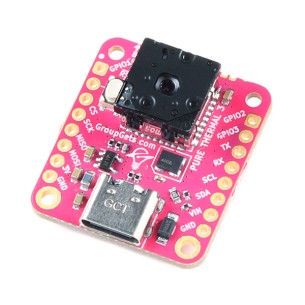
A set with an adapter dedicated to the FLIR Lepton thermal imaging camera and the Lepton FS camera. It has been pre-configured to operate as a plug-and-play UVC 1.0 USB camera, it can also communicate via UART and I2C interface. SparkFun DEV-20813
No product available!
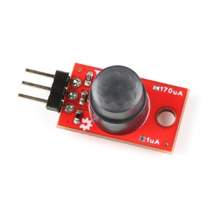
Motion detection module featuring Panasonic\'s EKM series PIR sensor. The EKM series is optimised for detecting small movements and is ideal for detecting movement in a small area around the sensor. It offers digital output in 32 zones with a detection distance of 5 m and a detection area of 90° x 90°. SparkFun SEN-22000
No product available!
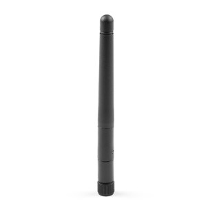
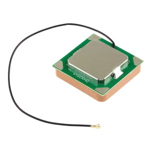
Antenna dedicated to communication in LoRa networks in the 868 MHz frequency band. Equipped with an RP-SMA connector. SparkFun WRL-18082
No product available!
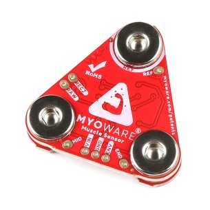
Sensor module for electromyography (EMG). Allows muscle activity to be studied and used to control devices. SparkFun DEV-21265
No product available!
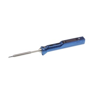
Portable soldering iron with a power of 65 W. It has an adjustable operating temperature in the range of 50 ° C to 400 ° C. It can be powered via a DC or USB type C connector. The set includes a soldering iron and a BC2 tip. MiniWare TS101 (BC2) Blue
No product available!
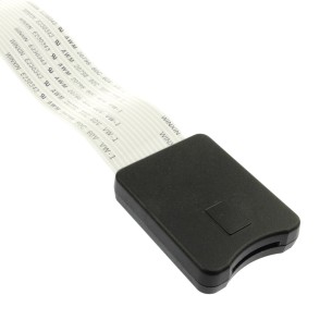
Flexible 25 cm microSD to SD adapter. Supports all card capacities and types including: 16GB, 32GB, 64GB, 128GB Micro SD/SDHC
No product available!
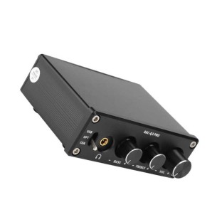
DAC converter with built-in headphone amplifier. It is powered by DC 5V/1A and can work with various power sources, ensuring operational stability and excellent sound quality. DAC-Q3 Pro
No product available!
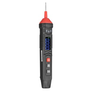
The digital meter with smart testing function is an advanced measuring device that offers a wide range of functions and capabilities. It is compact and portable and complies with safety standards for accurate and reliable measurement results.
No product available!
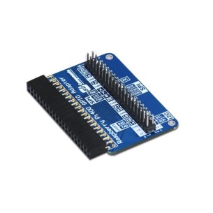
Expansion module designed to work with a portable computer built into the Raspberry Pi 400 keyboard. The board has a 40-pin connector in a vertical position. SB Components 21239
No product available!
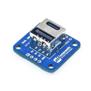
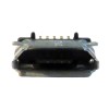
Module with USB type C and USB type A connectors designed for prototyping devices. The pins have been led out on the connector with a raster of 2.54 mm, which greatly facilitates the use of USB, e.g. with breadboards. SB Components 25756
No product available!
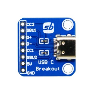
Module with USB type C connector designed for prototyping devices. The pins have been led out on the connector with a raster of 2.54 mm, which greatly facilitates the use of USB type C, e.g. with breadboards. SB Components 27330
No product available!
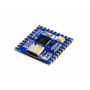
Board with RP2040 microcontroller equipped with two ARM Cortex-M0+ 133 MHz cores, 264 kB RAM. There is also 2 MB of QSPI flash memory on the board. The circuit can be programmed in C/C++, CircuitPython or MicroPython. SB Components 26531
No product available!
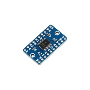
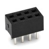
8-bit voltage level converter with TXB0108 integrated circuit. It acts as a bridge between applications with different source voltages and input and output voltage levels. SB Components 21772
No product available!
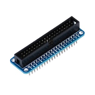
Adapter designed for Raspberry Pi minicomputers. It facilitates access to all pins, which are led out on the connector with a raster of 2.54 mm, which allows the use of a breadboard. SB Components 14927
No product available!