
- Out-of-Stock


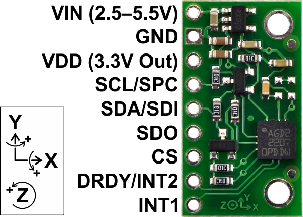
This sensor is a carrier/breakout board for the ST L3GD20 three-axis gyroscope, which measures the angular rates of rotation about the pitch (x), roll (y), and yaw (z) axes. Angular velocity measurements with a configurable range of ±250°/s, ±500°/s, or ±2000°/s can be read through a digital I2C or SPI interface. The board has a 3.3 V linear regulator and integrated level-shifters that allow it to work over an input voltage range of 2.5–5.5 V, and the 0.1” pin spacing making it easy to use with standard solderless breadboards and 0.1” perfboards.
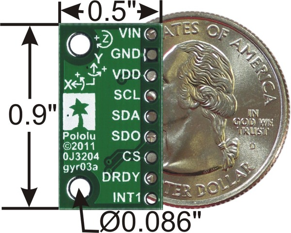 |
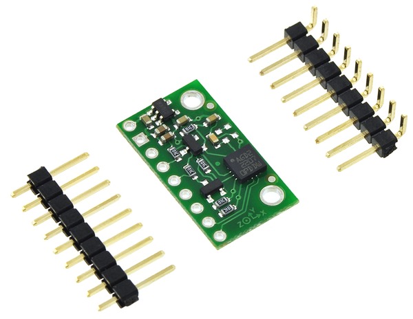
This board is a compact (0.5” × 0.9”) breakout board for ST’s L3GD20 three-axis digital-output gyroscope; we therefore recommend careful reading of the L3GD20 datasheet (2MB pdf) before using this product. The L3GD20 is a great IC, but its small, leadless, LGA package makes it difficult for the typical student or hobbyist to use. It also operates at voltages below 3.6 V, which can make interfacing difficult for microcontrollers operating at 5 V. This carrier board addresses these issues by incorporating additional electronics, including a 3.3 V voltage regulator and level-shifting circuits, while keeping the overall size as compact as possible. The board ships fully populated with its SMD components, including the L3GD20, as shown in the product picture.
Compared to the L3G4200D, the L3GD20 uses a higher resonant frequency that makes it more resistant to audio noise and vibrations. This board remains pin-compatible with the original L3G4200D carrier, although changes in I2C addresses and configuration registers mean that code written to interface with an L3G4200D might need to be modified to work with an L3GD20.
The L3GD20 has many configurable options, including three selectable angular rate sensitivities, a choice of output data rates, an embedded FIFO for buffering output data, and a programmable external interrupt signal. The three angular velocity readings are available through a digital interface, which can be configured to operate in either I2C or SPI mode.
The carrier board includes a low-dropout linear voltage regulator that provides the 3.3 V required by the L3GD20, which allows the sensor to be powered from a 2.5-5.5 V supply. The regulator output is available on the VDD pin and can supply almost 150 mA to external devices. The breakout board also includes a circuit that shifts the I2C/SPI clock and data in lines to the same logic voltage level as the supplied VIN, making it simple to interface the board with 5 V systems, and the board’s 0.1” pin spacing makes it easy to use with standard solderless breadboards and 0.1” perfboards.
For sensor fusion applications, our MinIMU-9 v2 inertial measurement unit combines the L3GD20 with an LSM303DLHC 3-axis accelerometer and 3-axis magnetometer on a board even smaller than this L3GD20 carrier, providing nine independent readings that can be used to calculate an absolute orientation.
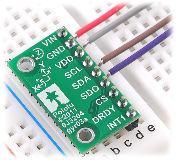
A 9×1 strip of 0.1” header pins and a 9×1 strip of 0.1” right-angle header pins are included, as shown in the picture below. You can solder the header strip of your choice to the board for use with custom cable or solderless breadboards, or you can solder wires directly to the board itself for more compact installations.
 |
Regardless of the interface being used to communicate with the L3GD20, its VIN pin should be connected to a 2.5-5.5 V source, and GND should be connected to 0 volts. (Alternatively, if you are using the gyro with a 3.3 V system, you can leave VIN disconnected and bypass the built-in regulator by connecting 3.3 V directly to VDD.)
A minimum of two logic connections are necessary to use the L3GD20 in I2C mode (this is the default mode): SCL and SDA. These should be connected to an I2C bus operating at the same logic level as VIN.
To use the L3GD20 in SPI mode, four logic connections are required: SPC, SDI, SDO, and CS. These should be connected to an SPI bus operating at the same logic level as VIN. The SPI interface operates in 4-wire mode by default, with SDI and SDO on separate pins, but it can be configured to use 3-wire mode so that SDO shares a pin with SDI.
|
|
| PIN | Description |
|---|---|
| VIN | This is the main 2.5-5.5 V power supply connection. The SCL/SPC and SDA/SDI level shifters pull the I2C and SPI bus high bits up to this level. |
| GND | The ground (0 V) connection for your power supply. Your I2C or SPI control source must also share a common ground with this board. |
| VDD | Regulated 3.3 V output. Almost 150 mA is available to power external components. (If you want to bypass the internal regulator, you can instead use this pin as a 3.3 V input with VIN disconnected.) |
| SCL/SPC | Level-shifted I2C/SPI clock line: HIGH is VIN, LOW is 0 V |
| SDA/SDI | Level-shifted I2C data line and SPI data in line (also doubles as SDO in 3-wire mode): HIGH is VIN, LOW is 0 V |
| SDO | SPI data out line in 4-wire mode: HIGH is VDD, LOW is 0 V. This output is not level-shifted. Also used as an input to determine I2C slave address (see below). |
| CS | SPI enable (chip select). Pulled up to VDD to enable I2C communication by default; drive low to begin SPI communication. |
| DRDY/INT2 | Data ready indicator, a 3.3-V-logic-level output. HIGH (3.3 V) indicates angular rate data can be read. Can also be configured as a FIFO interrupt. This output is not level-shifted. |
| INT1 | Programmable interrupt, a 3.3-V-logic-level output. This output is not level-shifted. |
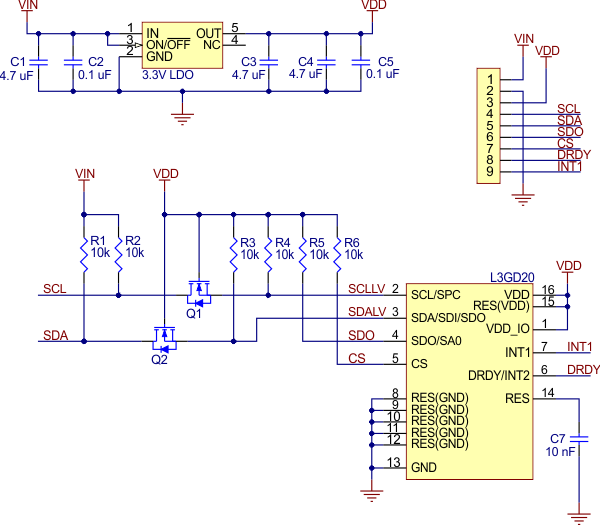 |
The above schematic shows the additional components the carrier board incorporates to make the L3GD20 easier to use, including the voltage regulator that allow the board to be powered from a 2.5-5.5 V supply and the level-shifter circuit that allows for I2C and SPI communication at the same logic voltage level as VIN.
With the CS pin in its default state (pulled up to VDD), the L3GD20 can be configured and its angular velocity readings can be queried through the I2C bus. Level shifters on the I2C clock (SCL) and data (SDA) lines enable I2C communication with microcontrollers operating at the same voltage as VIN (2.5-5.5 V).
In I2C mode, the gyro’s 7-bit slave address has its least significant bit (LSb) determined by the voltage on the SDO pin. The carrier board pulls SDO to VDD through a 10 k? resistor, making the LSb 1 and setting the slave address to 1101011b by default. If the gyro’s selected slave address happens to conflict with some other device on your I2C bus, you can drive SDO low to set the LSb to 0.
In our tests of the board, we were able to communicate with the chip at clock frequencies up to 400 kHz; higher frequencies might work but were not tested. The chip itself and carrier board do not meet of some requirements to make the device compliant with I2C fast-mode. It is missing 50 ns spike suppression on the clock and data lines, and additional pull-ups on the clock and data lines might also be necessary to achieve compliant signal timing characteristics.
To communicate with the L3GD20 in SPI mode, the CS pin (which the board pulls to VDD through a 10 k? resistor) must be driven low before the start of an SPI command and allowed to return high after the end of the command. Level shifters on the SPI clock (SPC) and data in (SDI) lines enable SPI communication with microcontrollers operating at the same voltage as VIN (2.5-5.5 V).
In the default 4-wire mode, the gyro transmits data to the SPI master on a dedicated data out (SDO) line. If the SPI interface is configured to use 3-wire mode instead, the SDI line doubles as SDO and is driven by the L3GD20 when it transmits data to the master.
We have written a basic Arduino library for the L3GD20 that makes it easy to interface this sensor with an Arduino. The library makes it simple to configure the L3GD20 and read the raw gyro data through I2C.
The datasheet provides all the information you need to use this sensor, but picking out the important details can take some time. Here are some pointers for communicating with and configuring the L3GD20 that we hope will get you up and running a little bit faster:
Download:
Manufacturer BTC Korporacja sp. z o. o. Lwowska 5 05-120 Legionowo Poland sprzedaz@kamami.pl 22 767 36 20
Responsible person BTC Korporacja sp. z o. o. Lwowska 5 05-120 Legionowo Poland sprzedaz@kamami.pl 22 767 36 20
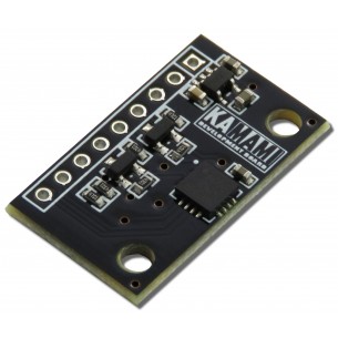
KAmodL3GD20 is a digital gyroscope module with L3GD20 chip. It makes possible to measure angular velocity up to ± 2000 degrees per second. It has a embedded voltage regulator and level translators on SDA/SCL lines, thanks to which it can be used in systems supplied with a voltage of 2.5 V-5.5 V. KAmodL3GD20
A kit for building a four-wheeled platform controlled by a mobile application. TMK-4WDU totem
No product available!
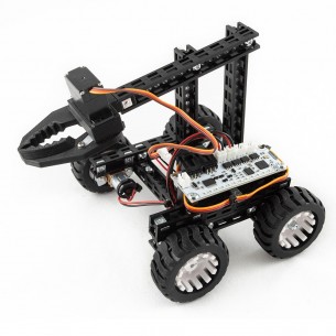
A set for building a mobile robot with a gripper controlled by a mobile application. TMK-DMNNG totem
No product available!
Kit for building a dog robot controlled by a wire with a switch. Totem TKR-DG
No product available!
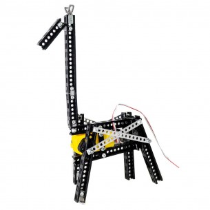
Kit for building a giraffe robot controlled by a wire with a switch. Totem TKR-GRF
No product available!
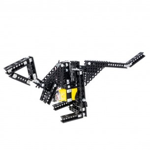
Kit for building a dinosaur robot controlled by a wire with a switch. Totem TKR-TRX
No product available!
A set for building a walking robot controlled by a mobile application. Totem TKR-LSP
No product available!
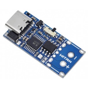
The trigger module is designed for chargers PD 2.0 and PD 3.0. It is equipped with a USB type C input and output on pads. It enables powering devices with 9 V or 12 V and testing chargers. PDC005
No product available!
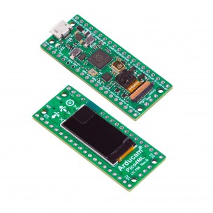
Development kit with RP2040 microcontroller equipped with two ARM Cortex-M0 + cores that work at 133 MHz, 264 kB RAM. The board has a QVGA camera, LCD display, IMU system and a microphone. ArduCAM B0302
No product available!
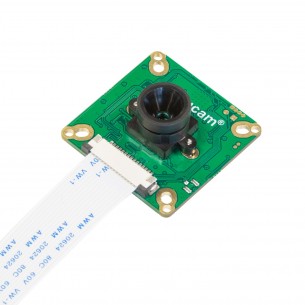
Camera module with a resolution of 13 MP equipped with an image sensor AR1335. It is equipped with a FoV 50° lens with an M12 mount. Designed for Raspberry Pi and Jetson Nano. ArduCAM B0277
No product available!
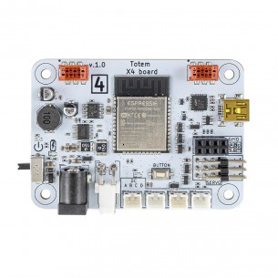
Robot controller dedicated to Totem sets. It is based on the ESP32 chip (WiFi and Bluetooth module), equipped with a DC motor and servo driver, RGB diodes and an IMU sensor. Totem TE-X4-KIT1
No product available!
Robot controller dedicated to Totem sets. It is equipped with Bluetooth communication, so it can be controlled using a smartphone. TMK-X3K totem
No product available!
Thermally conductive tape used as a replacement for thermally conductive paste. They are very flexible and characterized by high compressibility. AG Termopasty ART.AGT-161
No product available!
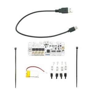
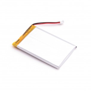
Li-Po battery with a rated voltage of 3.7 V and a capacity of 1350 mAh, equipped with a PCM protection and a 1.5 JST-ZH connector. Akyga LP503758
No product available!
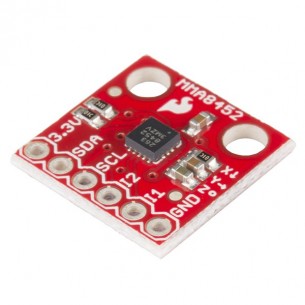
Module with a 3-axis MMA8452Q accelerometer. The system has a configurable measurement scale of ±2g/±4g/±8g. It is supplied with the voltage from 1.95 to 3.3 V and communicates via the I2C interface. SparkFun SEN-12756
No product available!
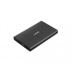
External enclosure designed to protect, transfer and store data on 2.5” HDD and SSD drives with SATA interface. UGO UKZ-1531
No product available!
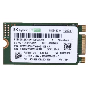
128 GB Hynix SSD. It is equipped with NVMe PCIe 3.0 interface with M.2 B&M Key connector. Hynix HFM128GDHTNG-8310A
No product available!