


- Out-of-Stock


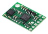
The LSM303DLM combines a digital 3-axis accelerometer and 3-axis magnetometer into a single package that is ideal for making a tilt-compensated compass. The six independent readings, whose sensitivities can be set in the ranges of ±2 to ±8 g and ±1.3 to ±8.1 gauss, are available through an I2C interface. This LSM303 carrier board includes voltage regulators and a level-shifting circuit that allows operation from 2.6 to 5.5 V, and the 0.1" pin spacing makes it easy to use with standard solderless breadboards and 0.1" perfboards.
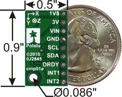 |
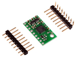
This board is a compact (0.5" ? 0.9") breakout board for ST’s LSM303DLM 3-axis accelerometer and 3-axis magnetometer; we therefore recommend careful reading of the LSM303DLM datasheet (519k pdf) before using this product. The LSM303DLM is a great IC, but its small package makes it difficult for the typical student or hobbyist to use. The device also requires multiple voltage supplies not typically available when interfacing with 3.3 or 5 V systems. This carrier board addresses these issues by incorporating additional electronics, including two voltage regulators and a level-shifting circuit, while keeping the overall size as compact as possible. The board ships fully populated with its SMD components, including the LSM303, as shown in the product picture.
The LSM303 has many configurable options, including dynamically selectable sensitivities for the accelerometer and magnetometer, a choice of output data rates, and two independently-programmable external inertial interrupt pins. The magnetometer and accelerometer can be individually turned on and off to save power, and a special sleep-to-wakeup function allows the accelerometer to sleep until an inertial interrupt is triggered. The six independent magnetic and acceleration readings (sometimes called 6DOF) are available through an I˛C/TWI interface and can be used for many applications, including making a tilt-compensated compass that can be used to determine headings regardless of how the board is inclined (ST provides an application note (1MB pdf) that explains the details of making one).
The carrier board includes two voltage regulators that provide the 1.8 V and 3 V required by the LSM303, which allows the sensor to be powered from a single 2.6 – 5.5 V supply. The regulator outputs are available on the 1V8 and 3V pins and can supply almost 150 mA and 300 mA, respectively, to external devices. The breakout board also includes a circuit that shifts the I˛C clock and data lines to the same logic voltage level as the supplied VIN, making it simple to interface the board with 3.3 V or 5 V systems, and the board’s 0.1" pin spacing makes it easy to use with standard solderless breadboards and 0.1" perfboards.
For sensor fusion applications, our MinIMU-9 inertial measurement unit combines the LSM303DLM with an L3G4200D 3-axis gyro on a board barely bigger than this LSM303DLM carrier alone, providing nine independent readings that can be used to calculate an absolute orientation.
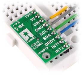
A 9?1 strip of 0.1" header pins and a 9?1 strip of 0.1" right-angle header pins are included, as shown in the picture below. You can solder the header strip of your choice to the board for use with custom cables or solderless breadboards, or you can solder wires directly to the board itself for more compact installations.
 |
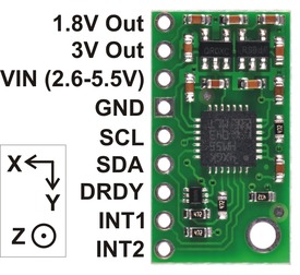
A minimum of four connections are necessary to use the LSM303DLM: VIN, GND, SCL, and SDA. VIN should be connected to a 2.6 – 5.5 V source, GND to 0 volts, and SCL and SDA should be connected to an I˛C bus operating at the same logic level as VIN.
|
|
| PIN | Description |
|---|---|
| VIN | This is the main 2.6 – 5.5 V power supply connection. The SCL and SDA level shifters pull the I˛C bus high bits up to this level. |
| GND | The ground (0 V) connection for your power supply. Your I˛C control source must also share a common ground with this board. |
| 1V8 | Regulated 1.8 V output. Almost 150 mA is available to power external components. |
| 3V | Regulated 3.0 V output. Almost 300 mA is available to power external components. |
| SCL | Level-shifted I˛C clock line: HIGH is VIN, LOW is 0 V |
| SDA | Level-shifted I˛C data line: HIGH is VIN, LOW is 0 V |
| DRDY | Magnetometer data ready indicator, a 1.8V-logic-level output. HIGH (1.8 V) indicates magnetometer data can be read. LOW (0 V) indicates the magnetometer is writing new data to the data registers. This output is not level-shifted. |
| INT1 | Inertial interrupt 1, a 1.8V-logic-level output. This output is not level-shifted. |
| INT2 | Inertial interrupt 2, a 1.8V-logic-level output. This output is not level-shifted. |
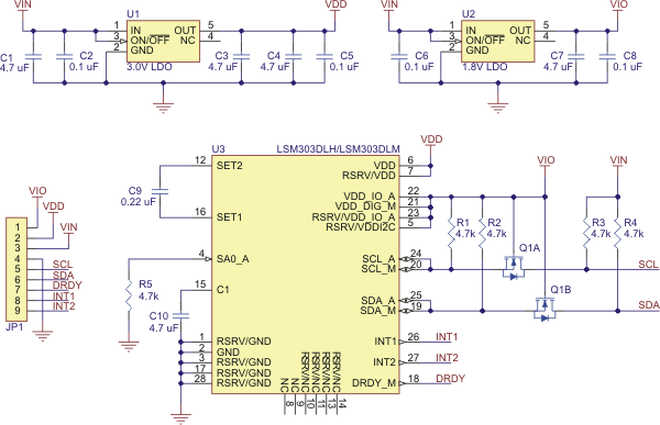 |
The above schematic shows the additional components the carrier board incorporates to make the LSM303 easier to use, including the voltage regulators that allow the board to be powered from a single 2.6 – 5.5 V supply and the level-shifter circuit that allows for I˛C communication at the same logic voltage level as VIN.
The LSM303DLM readings can be queried and the device can be configured through the I˛C bus. The module acts as two chained I˛C slave devices, with the accelerometer and magnetometer clock and data lines tied together to the same I˛C bus to ease communication. Additionally, level shifters on the I˛C clock (SCL) and data lines (SDA) enable I˛C communication with microcontrollers operating at the same voltage as VIN (2.6 – 5.5V). A detailed explanation of the protocol can be found in the LSM303DLM datasheet (519k pdf), and more detailed information about I˛C in general can be found in NXP’s I˛C-bus specification (371k pdf).
The accelerometer and the magnetometer have separate 7-bit slave addresses on the I˛C bus. The magnetometer’s slave address is 0011110b and cannot be changed. The accelerometer’s slave address has its least significant bit (LSb) determined by the voltage on the slave address selector pad (SA0_A). The carrier board pulls SA0_A to ground through a 4.7kΩ resistor, setting the accelerometer’s slave address to 0011000b by default. If the accelerometer’s selected slave address happens to conflict with some other device on your I˛C bus, it is possible to access SA0_A through the untented via on the bottom of the board and pull it up.
In our tests of the board, we were able to communicate with the chip at clock frequencies up to 400 kHz; higher frequencies might work but were not tested. The chip itself and carrier board do not meet of some requirements to make the device compliant with I˛C fast-mode. It is missing 50ns spike suppression on the clock and data lines, and additional pull-ups on the clock and data lines might also be necessary to achieve compliant signal timing characteristics.
The datasheet provides all the information you need to use this sensor, but picking out the important details can take some time. Here are some pointers for communicating with and configuring the LSM303DLM that we hope will get you up and running a little bit faster:
The inertial interrupts (INT1 and INT2) are highly configurable 1.8V-level outputs that can change due to accelerations (the magnetometer has no effect on INT1 or INT2). If the sleep-to-wakeup feature of the accelerometer is enabled, when an interrupt is triggered, the accelerometer wakes up.
 |
MinIMU-9 Gyro, Accelerometer, and Compass (L3G4200D and LSM303DLM Carrier) |
 |
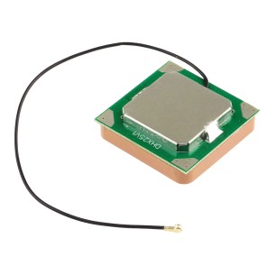
66-Channel LS20031 GPS Receiver Module |
 |
0.100" (2.54 mm) Breakaway Male Header: 1x40-Pin, Straight |
Manufacturer BTC Korporacja sp. z o. o. Lwowska 5 05-120 Legionowo Poland sprzedaz@kamami.pl 22 767 36 20
Responsible person BTC Korporacja sp. z o. o. Lwowska 5 05-120 Legionowo Poland sprzedaz@kamami.pl 22 767 36 20
No product available!
Micro SDHC 16GB class 10 UHS-I memory card with adapter
No product available!
No product available!
RoboClaw 2x45A Motor Controller (V5D) is a two-channel DC motor driver, operating voltage: 6-34V, maximum continuous current: 45A, easy implementation of feedback loops with PID controller, safety systems. Pololu 3287
No product available!
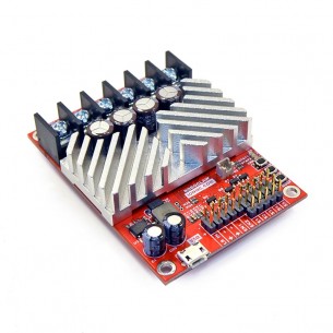
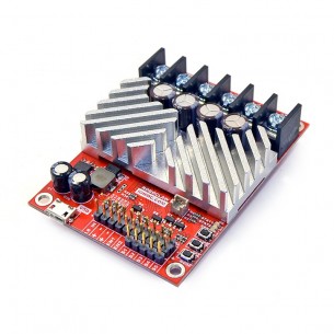
The RoboClaw motor controllers from Basicmicro (formerly Ion Motion Control) can control a pair of brushed DC motors using USB serial, TTL serial, RC or analog inputs. This version can supply a continuous 15 A per channel (30 A peak) and operates up to 34 V.
No product available!
The RoboClaw motor controllers from Basicmicro (formerly Ion Motion Control) can control a pair of brushed DC motors using USB serial, TTL serial, RC, or analog inputs. This version can supply a continuous 30 A per channel (60 A peak) and operates up to 34 V.
No product available!
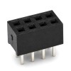
Pin strip straight in yellow, single-row, extended, female, 1x8, pitch 2.54mm, THT, RoHS. PB10S L YELLOW
No product available!
Pin strip straight in yellow, single-row, extended, female, 1x6, pitch 2.54mm, THT, RoHS. PB06S L YELLOW
No product available!
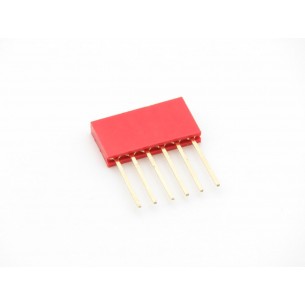
Pin strip straight in red, single-row, extended, female, 1x6, pitch 2.54mm, THT, RoHS. PB06S L RED
No product available!
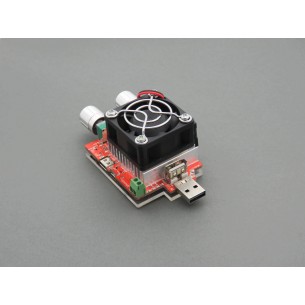
Adjustable USB load displaying voltage and current consumption of connected devices. The load can draw current up to 3 A. The voltage is measured in the range 3.5 ... 21V, current 0 ... 4A. It is also possible to measure cell capacity
No product available!
No product available!
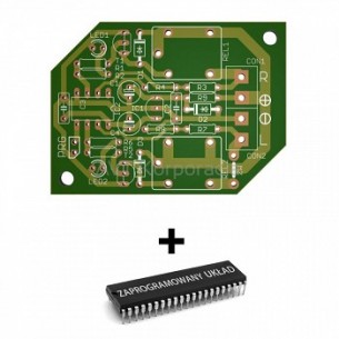
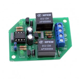
Printed circuit board and programmed layout for building a comfortable direction indicator module. AVT1945 A +
No product available!
AVT kit for self-assembly of the comfortable direction indicator module. AVT1945 B
No product available!
Assembled module of comfortable direction indicators. AVT1945 C
No product available!
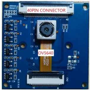
The camera V3 module is specifically designed for Banana Pi M3. Includes two CMOS sensor modules: OV5640 (5M Pixel) and OV8865(8M Pixel)
No product available!
Pin strip straight in blue, single-row, extended, female, 1x8, pitch 2.54mm, THT, RoHS. PB10S L BLUE
No product available!