


")
")

zł37,502.12 tax excl.
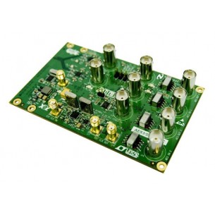
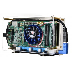
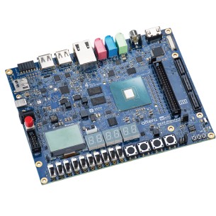
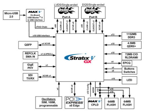
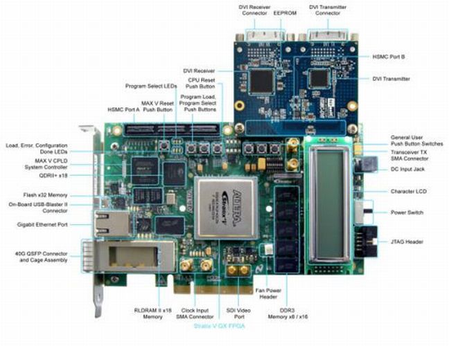
Stratix V GX FPGA Video Development System
Overview
The Stratix V GX FPGA Video Development System fills the need for the highest bandwidth, best performance video applications. The kit features an extensive feature-set of memories, including DDR3, QDRII+, and RLDRAM II. The QSFP optical cage, PCIe x8 edge connectors, SDI, and gigabit Ethernet options allow for blazingly fast interfacing with peripherals.
The DVI-HSMC daughter card part of the bundled package will allow developers to access high quality and high resolution video signals that can support resolution up to 1600x1200. A complete DVI video controller design with source code is provided.
Terasic recognized for its strong design expertise in high-end video, imaging and multimedia products have made available a video development package that targets video processing development. The platform can also allow users to experience advanced image processing designs incorporating VIP (Altera’s Video and Image Processing Suite MegaCore Functions).
Specification
Stratix V GX Video Development System
Terasic DVI-HSMC Card
Layout
Resources
Kit Contents
Demo
DVI Video Development System Bundle
The Terasic DVI Development System bundles together the DVI daughter card and Altera development kit for cost-effective video development. All source code shown is included.
Code: K0117
Manufacturer BTC Korporacja sp. z o. o. Lwowska 5 05-120 Legionowo Poland sprzedaz@kamami.pl 22 767 36 20
Responsible person BTC Korporacja sp. z o. o. Lwowska 5 05-120 Legionowo Poland sprzedaz@kamami.pl 22 767 36 20
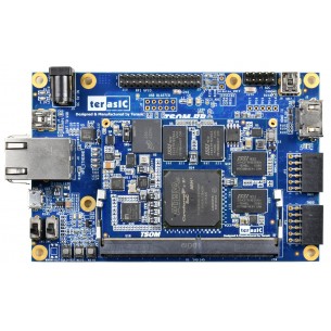
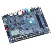
Integrated single board computer with Cyclone V SoC core. SoC SoM includes DDR3 memory, Flash memory, energy management system, common interface controllers and disc software (BSP). Terasic P0581
No product available!
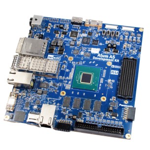
Terasic Atum A5 Development Kit – an advanced Intel Agilex 5 FPGA kit for AI, vision systems, and high-bandwidth applications. Terasic Atum A5 Development Kit
No product available!
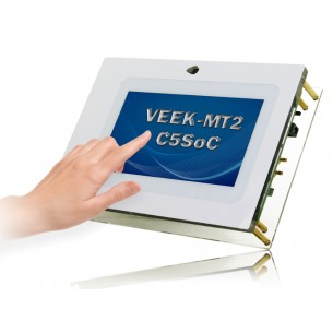
The Video and Embedded Evaluation Kit - Multi-touch, Second Edition, on Cyclone® V SoC Development Board (VEEK-MT2-C5SoC)
No product available!
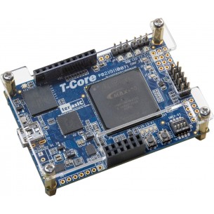
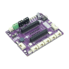
Development platform based on Intel MAX 10 FPGA. The system provides the user with 50,000 logical elements and 1638 kbits M9K and 5888 kbits Flash. The board contains components such as embedded USB-Blaster II, QSPI Flash, ADC connector, WS2812B RGB LED and 2x6 TMD connector. TerasiC T-Core P0633
No product available!
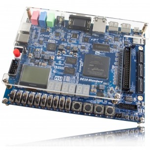
The DE10-Standard Development Kit presents a robust hardware design platform built around the Intel System-on-Chip (SoC) FPGA, which combines the latest dual-core Cortex-A9 embedded cores with industry-leading programmable logic for ultimate design flexibility. P0493
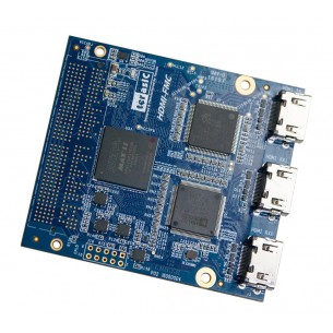
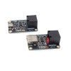
Terasic HDMI-FMC is a HDMI transmitter/receiver daughter board with FMC (FPGA Mezzanine card) interface
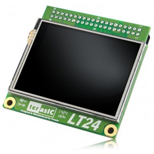
The Terasic LT24 is a 2.4” LCD touch module with 240(H) x 320(V) display resolution. It can be bundled with various Terasic FPGA development boards through the 2x20 GPIO interface. P0185
TerasIC SDI HSMC is a specialized module for FPGA projects in the field of video transmission, offering support for SDI and AES standards and full compatibility with HSMC platforms. It is ideal for developing broadcasting solutions, signal analyzers, and professional video applications.
TerasIC TR4-530 (P0109) is an FPGA development kit featuring the Stratix IV GX device, offering high logic performance, high-speed DDR3 memory support, and extensive expandability through HSMC and PCIe connectors. The platform is designed for prototyping digital systems, PCI Express applications, and real-time data processing.
No product available!
TerasIC TR4-230 (P0107) provides a development platform based on the Stratix IV GX FPGA, featuring a wide range of interfaces and support for PCI Express projects and high-speed DDR3 memory. The solution is designed for communication systems, ASIC prototyping, and applications requiring high logic resource capacity.
No product available!
The Terasic VEEK-MT2 set provides a complete hardware-software platform for designing embedded and multimedia systems using FPGA chips. It enables the creation and testing of interactive, control, and measurement applications thanks to an extensive base of interfaces, memory, and sensors.
No product available!
TerasIC DE0 is a complete evaluation kit based on the Cyclone III FPGA, designed for learning, testing, and implementing digital systems. It offers a wide range of interfaces and peripherals enabling the creation of complex projects for both educational and industrial purposes.
No product available!
FPGA starter kit equipped with Cyclone V GT with 301K LE and minicomputer with Intel Celeron Dual Core (64 GB eMMC, 4 GB RAM). The FPGA module has 1 GB DDR3 memory, 64 MB SDRAM memory, UART-USB interface and extensions such as GPIO and Arduino. Terasic P0650
No product available!
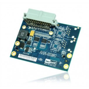
The TerasIC AHA-HSMC card enables the integration of Aptina image sensors with TerasIC FPGA kits equipped with an HSMC interface. It provides full support for communication, data transmission, and shutter control, making it a key component in vision systems and real-time image processing projects.
No product available!
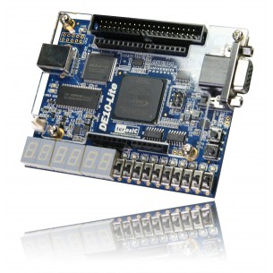
Terasic DE10-Lite is a cost-effective Altera MAX 10 based FPGA board. Kit contains lots of reference designs and software utilities for users to easily develop their applications based on these design resources
No product available!
Stratix V GX FPGA Video Development System