• Out-of-Stock
TerasIC A2GX-125 (K0036)
search
  • TerasIC A2GX-125 (K0036)
ID: 209396

Arria II GX Video Development System (with DVI+Software)

Retired
 

Free shipping

free shipping in Poland for all orders over 500 PLN


Same day shipping

If your payment will be credited to our account by 11:00


14 days for return

Each consumer can return the purchased goods within 14 days

TerasIC A2GX-125 (K0036) Arria II GX Video Development System (with DVI+Software)

Overview

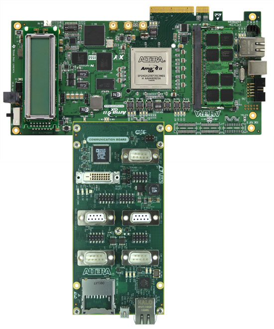
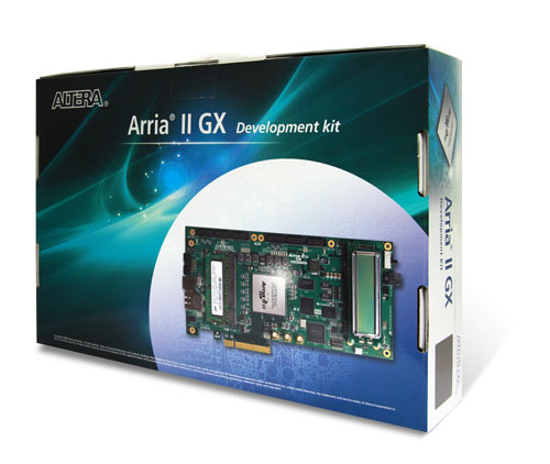
The Arria II GX Video Development System is an ideal video processing platform for high-end video applications.
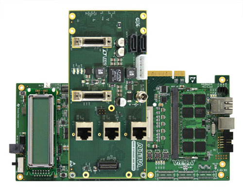
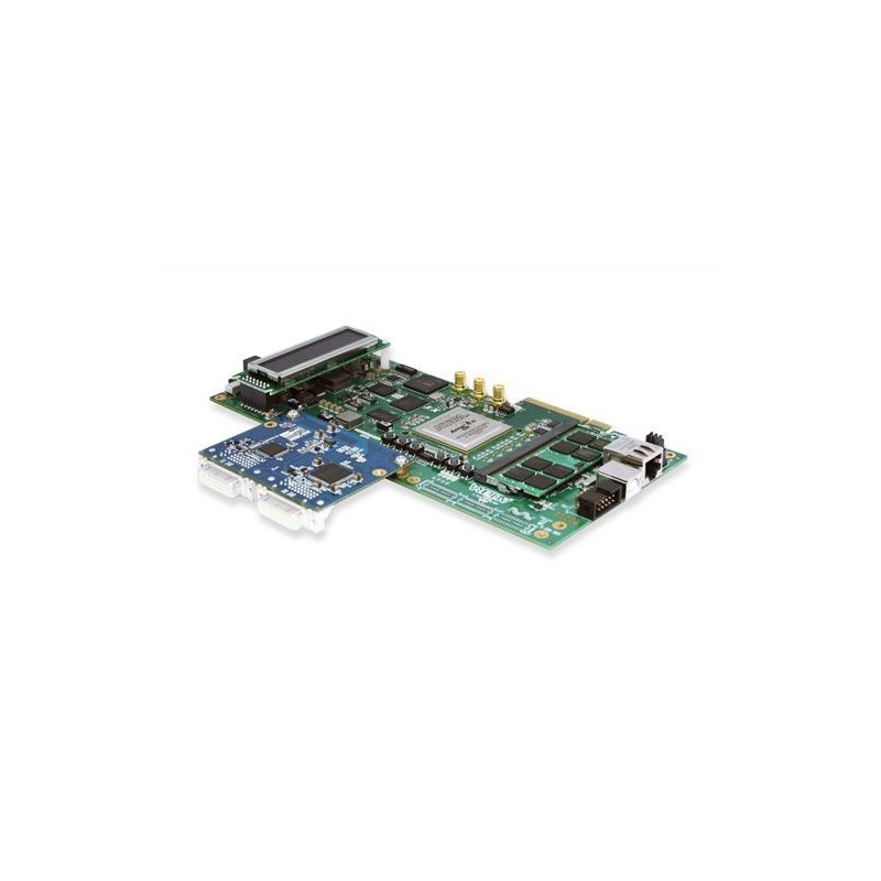
Terasic recognized for its strong design expertise in high-end video, imaging and multimedia products have made available a video development package that targets video processing development using an Arria II GX device. The package includes an Arria II GX FPGA development kit (DK-DEV-2AGX125N) featuring an EP2AGX FPGA device with HSMC connectors to allow additional functionality and connectivity via HSMC daughter boards. The Arria II GX FPGA development kit delivers a complete PCI Express-based development platform. This interface uses the Arria II GX device’s PCI Express hard IP to accelerate development time for high-volume PCI Express applications including add-in cards, host bus adapters, graphics cards, and high-end servers. Furthermore, the board includes an abundant amount of memory including on-board DDR3 device and DDR2 SODIMM, creating a complete integrated memory interface solution for memory-intensive applications.

The DVI-HSMC daughter card part of the bundled package will allow developers to access high quality and high resolution video signals that can support resolution up to 1600x1200. A complete DVI video controller design with source code is provided.

The development can also allow users to experience advanced image processing designs incorporating VIP (Altera’s Video and Image Processing Suite MegaCore Functions).

Specification

  • Arria II GX Development Board:
    • Arria II GX EP2AGX125EF35 FPGA
      • 124,100 logic elements (LEs)
      • 49,640 adaptive logic modules (ALMs)
      • 8,121 Kb on-chip memory
      • 12 high-speed transceivers
      • 6 phase-locked loops (PLLs)
      • 576 18x18 multipliers
      • 0.9V core power
    • Max® II EPM2210F256 CPLD
      • 2.5V core power
    • On-board ports
      • One HSMC expansion port
      • One gigabit Ethernet port
    • PCI Express x8 Edge Connector
      • Support connection speed of Gen1 at 2.5Gbps/lane
      • Connection established with PC motherboard with x8 PCI Express slot
    • On-board Memory
      • 128MB 16bit DDR3 device
      • 1GB 64bit DDR2 SO-DIMM
      • 2MB SSRAM
      • 64MB FLASH
    • FPGA Configuration Circuitry
      • MAX II CPLD and flash fast passive parallel configuration
      • On-board USB-Blaster™ circuitry using the Quartus II Programmer
    • On-board Clocking Circuitry
      • Four on-board oscillators
        • 100MHz
        • Programmable oscillator, default frequency 125MHz
        • Programmable oscillator, default frequency 100MHz
        • 155.52MHz
      • SMA connectors for external LVPECL clock input
      • SMA connector for clock output
    • General User I/O
      • LEDs/displays
        • Four user LEDs
        • Two-line character LCD display
        • One configuration-done LED
        • One HSMC interface transmit/receive LED (Tx/Rx)
        • Three PCI Express LEDs
        • Five Ethernet LEDs
    • Push-buttons
      • One user reset (CPU reset)
      • One MAX II CPLD reset
      • One load image (program FPGA from flash)
      • One image select (select image to load from flash)
      • Two general user push-buttons
    • DIP Switches
      • Four user DIP switches
      • Eight MAX II device control DIP switches
    • Power Supply
      • 14V to 20V DC input
      • PCI Express edge connector power
      • On-board power measurement circuitry
    • Arria II GX FPGA Development Kit CD-ROM
      • Design examples
        • Board Update Portal, featuring the Nios® II processor web server and remote system update
        • Board test system
    • Alteras Complete Design Suite DVD
      • Quartus II Software Development Kit Edition, includes support for Arria II GX FPGAs
      • Nios II Embedded Design Suite
      • MegaCore® IP Library includes PCI Express, Triple Speed Ethernet, SDI, and DDR3 High-Performance Controller IP cores
        • IP evaluation available through OpenCore Plus
  • DVI-HSMC Card:
    • Digital Transmitter
      • One DVI transmitter with single transmitting port
      • Digital Visual Interface (DVI) Compliant
      • Supports resolutions from VGA to UXGA (25 MHz – 165 MHz Pixel Rates)
      • Universal Graphics Controller Interface
        • 12-Bit, Dual-Edge and 24-Bit, Single-Edge Input Modes
        • Adjustable 1.1 V to 1.8 V and Standard 3.3 V CMOS Input Signal Levels
        • Fully Differential and Single-Ended Input Clocking Modes
        • Standard Intel 12-Bit Digital Video Port Compatible as on Intel™ 81x Chipsets
      • Enhanced PLL Noise Immunity
        • On-Chip Regulators and Bypass Capacitors for Reducing System Costs
      • Enhanced Jitter Performance
        • No HSYNC Jitter Anomaly
        • Negligible Data-Dependent Jitter
        • Programmable Using I2C Serial Interface
        • Single 3.3-V Supply Operation
    • Digital Receiver
      • One DVI receiver with single receiving port
      • Supports UXGA Resolution (Output Pixel Rates Up to 165 MHz)
      • Digital Visual Interface (DVI) Specification Compliant

Connect COMM


Layout

  • A2GX Development Board - 216X107 mm
  • DVI daughter card - 41 x 78.11 mm

Resources

Kit Contents


209396

Responsible person BTC Korporacja sp. z o. o. Lwowska 5 05-120 Legionowo Poland sprzedaz@kamami.pl 22 767 36 20

Other products in the same category (16)