


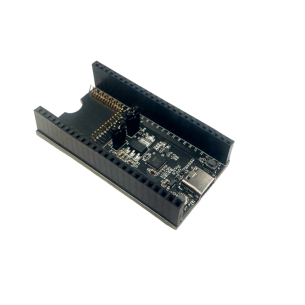
- Out-of-Stock


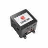
Xilinx Virtex-5 LXT ML555 FPGA Development Kit for PCI Express, PCI-X, and PCI Interfaces
HW-V5-ML555-G - Xilinx Virtex-5 LXT ML555 FPGA Development Kit for PCI Express, PCI-X, and PCI Interfaces
The Virtex™-5 LXT FPGA Development kit for PCI-Express® supports PCIe®/PCI-X™/PCI™. This complete development kit passed PCI-SIG compliance for PCI Express v1.1 and enables you to rapidly create and evaluate designs using PCI Express, PCI-X and PCI interfaces.
Key Features:
Content:
Module with a 3-axis ADXL356C accelerometer with a measuring range up to ± 40g. The board is equipped with a Grove connector and communicates via the analog interface. Seeed Studio 101020638
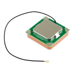
No product available!
Module with a 3-axis ADXL357 accelerometer with a measuring range up to ± 40g. The board is equipped with a Grove connector and communicates via the I2C interface. Seeed Studio 101020639
No product available!
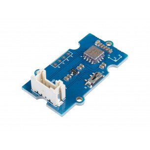
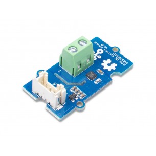
The module with the ACS725 current sensor with a direct current measuring range up to 10 A. The board is equipped with a Grove connector and communicates via an analog interface. Seeed Studio 101020616
No product available!
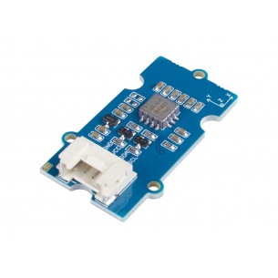
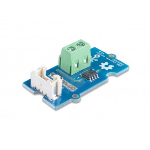
The module with the ACS70331 current sensor with a direct and alternating current measuring range ±5 A. The board is equipped with a Grove connector and communicates via an analog interface. Seeed Studio 101020615
No product available!
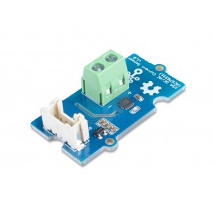
The module with the ACS70331 current sensor with a direct current measuring range up to 2,5 A. The board is equipped with a Grove connector and communicates via an analog interface. Seeed Studio 101020652
No product available!
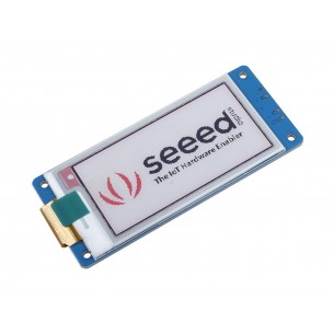
Module with a 3-color (red, black, white) e-Paper display with a diagonal of 1.54" and a resolution of 152x152 px. The board is equipped with a Grove connector and communicates via the UART interface. Seeed Studio 104020129
No product available!
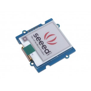
Module with a 3-color (red, black, white) e-Paper display with a diagonal of 2.13" and a resolution of 212x104 px. The board is equipped with a Grove connector and communicates via the UART interface. Seeed Studio 104020130
No product available!
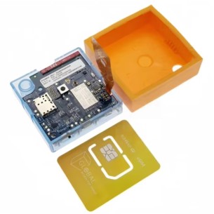
GPS tracking device (Tracker) with LoRa SX1276/1278 module and 9-axis IMU MPU9250. Seeed Studio 113990659
No product available!
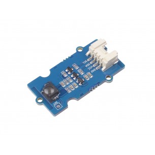
Module with IR motion sensor AK9753. The board is equipped with a Grove connector and communicates via the I2C interface. Seeed Studio 101020554
No product available!
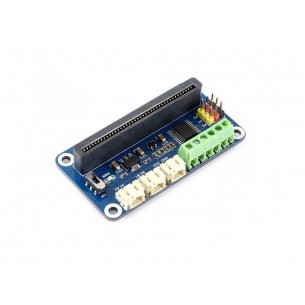
The module with the driver of 2 DC motors TB6612FNG and 3 servos, designed for the educational micro:bit module. Seeed Studio 105990091
No product available!
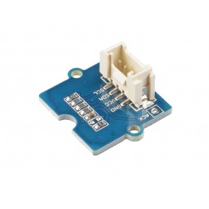
Module with a UV light sensor VEML6070. The board is equipped with a Grove connector and communicates via I2C. Seeed Studio 101020600
No product available!
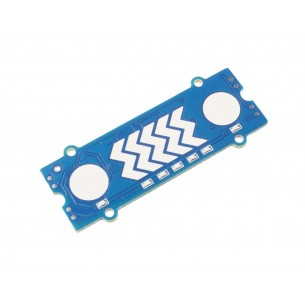
The module with the CY8C4014LQI touch sensor in the form of two buttons and a 5-segment slider. The board is equipped with a Grove connector and communicates via I2C. Seeed Studio 101020552
No product available!
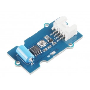
Module with vibration sensor SW-420. The board is equipped with a Grove connector and has a digital output. Seeed Studio 101020586
No product available!
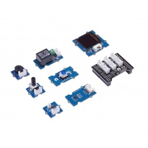
Starter kit with Grove modules designed to work with the Azure Sphere MT3620 development board. Seeed Studio 110060947
No product available!
Module with 5-way joystick. The board is equipped with a Grove connector and communicates via I2C. Seeed Studio 111020048
No product available!
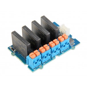
Module with 4 relays SSR G3MC202P with a load up to 2 A. The board is equipped with a Grove connector and communicates via I2C. Seeed Studio 103020135
No product available!
Xilinx Virtex-5 LXT ML555 FPGA Development Kit for PCI Express, PCI-X, and PCI Interfaces