
- Out-of-Stock


Baranowski J.
Extensive set of tasks with solutions, being an extension of the manual "Electronic circuits, Part 2 Nonlinear and pulsed analogue circuits", compatible with the program "Electronic circuits". The collection is aimed at introducing various electronic methods, both simpler and complex, to various methods of analysis. To solve these problems, the authors used both analytical calculation methods ("manual" calculations) and methods of computer analysis using NAP and PSPICE programs. A collection richly illustrated with the results of computer simulations.
The book is intended for students of the faculties of electronics and telecommunications of technical colleges
Table of Contents
LIST OF IMPORTANT MARKINGS
1. MULTILATERAL MODELS OF SEMICONDUCTOR ELEMENTS
1.1. Constant current diode model PN / 16
1.2. Operating point of the PN / 18 diode
1.3. Thermal dependence of the PN / 21 diode characteristics
1.4. Constant current Ebers-Molla model of the bipolar transistor / 21
1.5. Static analysis of the system with a bipolar transistor / 24
1.6. Temperature dependence of voltage on Zener diode / 28
1.7. Static and dynamic characteristics of a bipolar transistor with quasi-indication / 33
1.8. Static characteristics of the differential amplifier with NJFET / 47 transistors
1.9. The influence of the substrate on the static characteristics of the MOSFET / 58 transistor
1.10.Model diody ładunkowej / 71
2. SWITCHING OF SEMICONDUCTOR ELEMENTS
2.1. Switching diode / 85
2.2. Switching the diode stopper / 88
2.3. Two-stroke pulsed DC voltage converter / 94
2.4. Switching the bipolar transistor / 98
2.5. Switching of a bipolar transistor with capacitance / 102
2.6. Bipolar key loaded with relay / 104
2.7. Switching of a bipolar transistor with diode and accelerating capacity / 108
2.8. Switching of a bipolar transistor with respect to quasinancing / 112
2.9. Switching CMOS / 116 inverter
2.10. Dependency of the CMOS inverter on the supply voltage / 120
3. BASIC LOGIC GATES
3.1. Static characteristics of the TTL / 124 gate
3.2. Static characteristics of the TTL LS / 130 gate
3.3. Power consumed by the TTL LS / 132 gate
3.4. Power consumed by the TTL ALS / 133 gate
3.5. ECL gate from the MECL 10K / 134 family
3.6. ECL gateway from the 9500/137 family
3.7. Transient characteristics of the NMOS / 139 inverter
3.8. Switching NMOS inverter J 142
3.9. Transient characteristics of the NDMOS / 147 inverter
3.10. Switching of the NDMOS / 150 inverter
3.11. Transient characteristics of the CMOS / 157 inverter
3.12. Switching CMOS / 160 inverter
3.13. Static analysis of the CMOS inverter using the PSPICE / 165 simulator
4. QUICK ARRANGEMENT SYSTEMS
4.1. Shaping of pin impulses in the RC / 167 system
4.2. Shaping of pin impulses using a long line / 174
4.3. Shaping of sinusoidal impulses from a sinusoid using a charge diode / 180
4.4. Shaping the pulse edge using a load diode / 187
4.5. Compression ratio in nonlinear line / 192
4.6. Dependence of the compression ratio in the nonlinear line on the diode / 194 parameters
4.7. Compression ratio in a non-linear line as a function of the diode / 196 connector capacity
4.8. Dzielnik rezystancyjny /
5. ANALOG FUNCTIONAL SYSTEMS
5.1. Szybki układ próbkująco-pamiętający / 206
5.2. System próbkująco-pamiętający / 211
5.3. Detektor szczytowy / 214
5.4. Peak detector cooperating with resonant circuit / 216
5.5. Voltage multiplier as a power supply / 218
5.6. High voltage transformer / 223
5.7. Comparison of an operational amplifier with a comparator at large signals / 226
5.8. Multiplier as amplitude modulator / 231
5.9. Multiplier as an amplitude modulator with constant current coupling / 238
5.10. Quadrotor multiplier as an amplitude modulator with total suppression of carrier / 240
5.11. Multiplier as a synchronous detector / 246
5.12. Multiplier system with RC4200 / 251 chip
5.13. Miller integrator as a stepwise time base system / 253
5.14. Gateway transmission / 257
6. IMPULSE AND BROADBAND AMPS OF LARGE SIGNALS
6.1. Bipolar resistor in impulse application / 261
6.2. High-speed current / voltage converter / 266
6.3 Differential amplifier as broadband amplifier for large signals / 275
6.4. Wzmacniacz wizyjny / 285
6.5. Amplifier with current coupling / 297
7. GENERATORS OF SINUSOIDAL VIBRATIONS
7.1. Hartley generator with bipolar NPN transistor in WB configuration with capacitive load / 300
7.2. Colpitts generator with bipolar NPN transistor in VVB 309 configuration
7.3. Hartley generator with bipolar NPN transistor in WE / 314 configuration
7.4. Hartley generator with NJFET / 323 field effect transistor
7.5. Coefficient of regeneration in generators with transistors in the WC and WD / 331 configuration
7.6. Hartley generator with NJFET transistor in WD / 334 configuration
7.7. Colpitts generator with NJFET / 340 field effect transistor
7.8. Clapp generator with NJFET / 347 field effect transistor
7.9. Clapp generator with NJFET field effect transistor and high inductance coil / 355
7.10. Generator with negative resistance with bipolar transistors / 359
7.11. Quartz generator with NJFET / 364 field effect transistor
8. ASTABILE OVERVIEWS AND VCO SYSTEMS
8.1. Characteristics of a negative resistors / 374
8.2. Astacid transducer with modeled negative resistance / 378
8.3. Schmitt trigger and Miller integrator in the generator / 382 system
8.4. VCO system with Miller integrator and monostable bias / 385
8.5. Generator of a rectangular and triangular wave with the Schmitt / 386 trigger
8.6. Current generator / 388
8.7. Voltage-tuned generator (VCO) with NE565 / 391 system
9. MONOSTABLE FLEECE
9.1. Monostable bias in a quasi-symmetrical system / 397
9.2. Monostable relay in the Bowesa / 401 system
9.3. Monostable earthing with TTL / 405 gates
9.4. Monostable relay in the Schmitt / 409 system
9.5. Monostable earthing with element with non-linear resistance type S / 413
9.6. Monostable bias with diode tunnel / 418
9.7. Monostable bias with integrated circuit 74121/423
9.8. Monostable bias with 555/424 integrated circuit
10. BISTABILN VICTIMPERS
10.1. Static analysis of trigger triggered by level / 427
10.2. Static analysis of the trigger triggered / 430
10.3. Bistable latch with a negative biode type N / 435
10.4. Frequency divider with type D / 437 trigger
10.5. Toggle latch / 440
10.6. Comparator with regeneration / 444
11. PULSE POWER SUPPLIES
11.1. Simple impulse power supply / 448
11.2. Pulse voltage stabilizer with bi-directional keys / 453
11.3. Stabilized switching power supply in counter-current system / 458
11.4. Stabilized switching power supply in half-bridge / 462
11.5. Pulsed DC power supply implemented in the C-technology switched / 468
11.6. Pulse stabilizer with variable frequency keying / 472
12. SYSTEMS WITH PHASE LOOP COVER PLY
12.1. Characteristics of the phase detector / 480
12.2. The scope of holding the PLL / 483 loop
12.3. PLL system as a frequency multiplier and FM / 484 modulator
12.4. PLL layout as a filter / 493
12.5. FM demodulator with PLL / 498 chip
12.6. Sensitivity and internal frequency deviation of FM demodulator with PLL / 503 system
LITERATURE
No product available!
No product available!
Computer Raspberry Pi, I2C, SPI, 8IO, UART, LCD interface, Joystick, 8 LED, RoHS
No product available!
The SPWF01SA intelligent Wi-Fi modules represent a plug-and-play and standalone 802.11 b/g/n solution for easy integration of wireless internet connectivity features into existing or new products.
No product available!
No product available!
No product available!
No product available!
No product available!
No product available!
No product available!
No product available!
No product available!
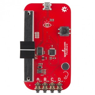
The PicoBoard allows you to create interactions with various sensors. Designed for educators and beginners, the PicoBoard is a good way to get into the very basics of programming and reading sensors. WIG-11888
No product available!
No product available!
No product available!
No product available!
Baranowski J.