

zł55.55 tax excl.
The LSM6DS33 combines a digital 3-axis accelerometer and 3-axis gyroscope into a single package. The sensor provides six independent acceleration and rotation rate readings whose sensitivities can be set in the ranges of ±2 g to ±16 g and ±125°/s to ±2000°/s, available through I²C and SPI interfaces.
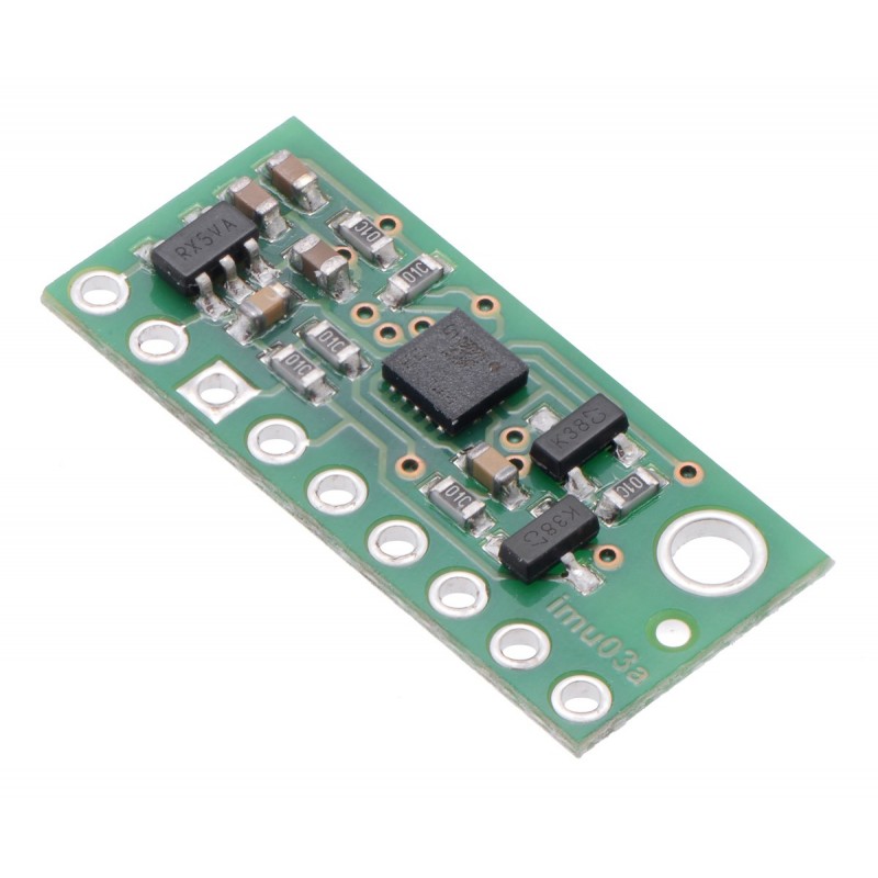
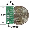
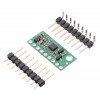
This board is a compact (0.4″ × 0.9″) breakout board for ST’s LSM6DS33 inertial module, which features a 3-axis digital linear accelerometer and 3-axis digital rate gyroscope; we therefore recommend careful reading of the LSM6DS33 datasheet (1MB pdf) before using this product. The LSM6DS33 is a great IC, but its small package makes it difficult for the typical student or hobbyist to use. It also operates at voltages below 3.6 V, which can make interfacing difficult for microcontrollers operating at 5 V. This carrier board addresses these issues by incorporating additional electronics, including a 3.3 V voltage regulator and level-shifting circuits, while keeping the overall size as compact as possible. The board ships fully populated with its SMD components, including the LSM6DS33, as shown in the product picture.
The LSM6DS33 inertial measurement unit (IMU) has many configurable options, including dynamically selectable sensitivities for the accelerometer and gyro, a choice of output data rates, and two independently-programmable external inertial interrupt pins. The accelerometer and gyro can be individually turned on and off to save power. The sensor can be configured and its readings can be accessed through a digital interface, which can be configured to operate in either I²C (TWI) or SPI mode.
The six independent acceleration and angular rate readings (sometimes called 6DOF) provide data that a microcontroller or computer can use to calculate the orientation of the LSM6DS33 on two axes (roll and pitch; a magnetometer is generally required to compute yaw accurately). With an appropriate algorithm, the gyro can be used to very accurately track rotation on a short timescale, while the accelerometer can help compensate for gyro drift over time by providing an absolute frame of reference.
The carrier board includes a low-dropout linear voltage regulator that provides the 3.3 V required by the LSM6DS33, which allows the sensor to be powered from a 2.5-5.5 V supply. The regulator output is available on the VDD pin and can supply almost 150 mA to external devices. The breakout board also includes a circuit that shifts the I²C clock and data lines to the same logic voltage level as the supplied VIN, making it simple to interface the board with 5 V systems, and the board’s 0.1″ pin spacing makes it easy to use with standard solderless breadboards and 0.1″ perfboards.
This LSM6DS33 carrier is pin-compatible with many of our previous ST I²C/SPI sensor carriers, including our LSM303D compass and accelerometer carrier and L3GD20H gyro carrier, and the orientation of the sensor axes is the same. However, since the ICs contain different sensors with different I²C addresses and configuration registers, code written to interface with another chip will need to be modified to work with an LSM6DS33.
For sensor fusion applications, our MinIMU-9 v5 and AltIMU-10 v5 inertial measurement units combine this LIS3MDL with an LSM6DS33 3-axis accelerometer and 3-axis gyro on a single board, providing nine independent readings that can be used to calculate an absolute orientation. The AltIMU-10 v5 also includes an LPS25H pressure sensor that can be used to calculate altitude.
A 1×9 strip of 0.1″ header pins and a 1×9 strip of 0.1″ right-angle header pins are included, as shown in the picture below. You can solder the header strip of your choice to the board for use with custom cables or solderless breadboards, or you can solder wires directly to the board itself for more compact installations.
Regardless of the interface being used to communicate with the LSM6DS33, its VIN pin should be connected to a 2.5 V to 5.5 V source, and GND should be connected to 0 volts. (Alternatively, if you are using the board with a 3.3 V system, you can leave VIN disconnected and bypass the built-in regulator by connecting 3.3 V directly to VDD.)
A minimum of two logic connections is necessary to use the LSM6DS33 in I²C mode (this is the default mode): SCL and SDA. These pins are connected to built-in level-shifters that make them safe to use at voltages over 3.3 V; they should be connected to an I²C bus operating at the same logic level as VIN. The remaining pins are not connected to level-shifters on the board and are not 5V-tolerant, but our 4-channel bidirectional logic level shifter can be used externally with those pins to achieve the same effect.
To use the LSM6DS33 in SPI mode, four logic connections are typically used: SPC, SDI, SDO, and CS. These should be connected to an SPI bus operating at the same logic level as VIN. The SPI interface operates in 4-wire mode by default, with SDI and SDO on separate pins, but it can be configured to use 3-wire mode so that SDO shares a pin with SDI.
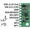
| PIN | Description |
|---|---|
| VDD | Regulated 3.3 V output. Almost 150 mA is available to power external components. (If you want to bypass the internal regulator, you can instead use this pin as a 3.3 V input with VIN disconnected.) |
| VIN | This is the main 2.5 V to 5.5 V power supply connection. The SCL/SPC and SDA/SDI level shifters pull the I²C and SPI bus high bits up to this level. |
| GND | The ground (0 V) connection for your power supply. Your I²C or SPI control source must also share a common ground with this board. |
| SDA/SDI/SDO | Level-shifted I²C data line and SPI data in line (also doubles as SDO in 3-wire mode): HIGH is VIN, LOW is 0 V |
| SCL/SPC | Level-shifted I²C/SPI clock line: HIGH is VIN, LOW is 0 V |
| SDO/SA0 | SPI data out line in 4-wire mode: HIGH is VDD, LOW is 0 V. This output is not level-shifted. Also used as an input to determine I²C slave address (see below). |
| CS | SPI enable (chip select). Pulled up to VDD to enable I²C communication by default; drive low to begin SPI communication. |
| INT2 | Programmable interrupt, a 3.3-V-logic-level output. This output is not level-shifted. |
| INT1 | Programmable interrupt, a 3.3-V-logic-level output. This output is not level-shifted. |
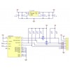
The above schematic shows the additional components the carrier board incorporates to make the LSM6DS33 easier to use, including the voltage regulator that allows the board to be powered from a single 2.5-5.5 V supply and the level-shifter circuit that allows for I²C and SPI communication at the same logic voltage level as VIN. This schematic is also available as a downloadable PDF (89k pdf).
With the CS pin in its default state (pulled up to VDD), the LSM6DS33 can be configured and its readings can be queried through the I²C bus. Level shifters on the I²C clock (SCL) and data lines (SDA) enable I²C communication with microcontrollers operating at the same voltage as VIN (2.5-5.5V). A detailed explanation of the protocol can be found in the LSM6DS33 datasheet (1MB pdf), and more detailed information about I²C in general can be found in NXP’s I²C-bus specification (1MB pdf).
In I²C mode, the sensor’s 7-bit slave address has its least significant bit (LSb) determined by the voltage on the SA0 pin. The carrier board pulls SA0 to VDD through a 10 kΩ resistor, making the LSb 1 and setting the slave address to 1101011b by default. If the selected slave address happens to conflict with some other device on your I²C bus, or if you want to use two LSM6DS33 sensors on the same bus, you can drive SA0 low to set the LSb to 0 (which sets the slave address to 1101010b).
The I²C interface on the LSM6DS33 is compliant with the I²C fast mode (400 kHz) standard. In our tests of the board, we were able to communicate with the chip at clock frequencies up to 400 kHz; higher frequencies might work but were not tested.
To communicate with the LSM6DS33 in SPI mode, the CS pin (which the board pulls to VDD through a 10 kΩ resistor) must be driven low before the start of an SPI command and allowed to return high after the end of the command. Level shifters on the SPI clock (SPC) and data in (SDI) lines enable SPI communication with microcontrollers operating at the same voltage as VIN (2.5 V to 5.5 V).
In the default 4-wire mode, the sensor transmits data to the SPI master on a dedicated data out (SDO) line that is not level-shifted. If the SPI interface is configured to use 3-wire mode instead, the SDI line doubles as SDO and is driven by the LSM6DS33 when it transmits data to the master. A detailed explanation of the SPI interface on the LSM6DS33 can be found in its datasheet (1MB pdf).
We have written a basic Arduino library for the LSM6 that makes it easy to interface this sensor with an Arduino or Arduino-compatible board like an A-Star. The library makes it simple to configure the LSM6DS33 and read the raw accelerometer and gyro data through I²C.
The datasheet provides all the information you need to use this sensor, but picking out the important details can take some time. Here are some pointers for communicating with and configuring the LSM6DS33 that we hope will get you up and running a little bit faster:
| Size: | 0.4″ × 0.9″ × 0.1″1 |
|---|---|
| Weight: | 0.6 g1 |
| Interface: | I²C, SPI2 |
|---|---|
| Minimum operating voltage: | 2.5 V |
| Maximum operating voltage: | 5.5 V |
| Measurement range: | ±2, ±4, ±8, or ±16 g (accelerometer) ±125, ±245, ±500, ±1000, or ±2000°/s (gyro)3 |
| Supply current: | 2 mA |
| PCB dev codes: | imu03a |
|---|---|
| Other PCB markings: | 0J9471 |
Data sheet
Manufacturer BTC Korporacja sp. z o. o. Lwowska 5 05-120 Legionowo Poland sprzedaz@kamami.pl 22 767 36 20
Responsible person BTC Korporacja sp. z o. o. Lwowska 5 05-120 Legionowo Poland sprzedaz@kamami.pl 22 767 36 20
Module with a 6-axis IMU sensor (accelerometer and gyroscope) that allows you to measure acceleration and rotational speed in a wide range of ±30g and ±4000dps. Communicates via I2C. Adafruit 4464
No product available!
A compact 9-DOF sensor that combines a 3-axis accelerometer, magnetometer, and gyroscope to precisely determine an object\'s orientation. With support for the I2C/SPI bus, compatibility with the STEMMA QT system, and 3V/5V power supply, it is suitable for robotics, 3D navigation, VR, AR, and stabilization systems. Adafruit 4634
No product available!
Module with 9-axis IMU dedicated to Feather plates. It connects the ISM330DHCX (accelerometer and gyroscope) and LIS3MDL (magnetometer) systems. Communication via the I2C interface. Adafruit 4569
Module with acceleration and rotational speed sensor based on the MPU6050 system. It communicates via the I2C or UART interface
No product available!
A module with an acceleration and rotational speed sensor based on the ICG-20660L system. It communicates via the I2C or SPI interface. DFRobot SEN0443
Module with 9-axis IMU ICM-20948 sensor (3-axis accelerometer, gyroscope and magnetometer and DMP) and BMP280 pressure sensor. Communication via I2C. Waveshare 10 DOF IMU Sensor (D)
No product available!
Module with 6-axis IMU sensor that allows you to measure acceleration and rotational speed in the range up to ±16g and ±2000dps. Equipped with a STEMMA QT connector, it communicates via I2C or SPI. Adafruit 4503
Module with 3-axis accelerometer and ISM330DHCX gyroscope. Equipped with a Qwiic connector, it communicates via the I2C or SPI interface. SparkFun SEN-19764
Module with 3-axis accelerometer and ISM330DHCX gyroscope. Equipped with a Qwiic connector, it communicates via the I2C interface. SparkFun SEN-20176
No product available!
A module with an acceleration and rotational speed sensor based on the LSM6DS3TR-C system and the LIS3MDL magnetometer. Equipped with a STEMMA QT connector, it communicates via the I2C or SPI interface. Adafruit 5543
Module with 9-axis IMU. It combines the ISM330DHCX (accelerometer and gyroscope) and MMC5983MA (magnetometer) systems. Communication via the I2C interface. SparkFun SEN-19895
No product available!
Small 10 DoF IMU module with 3-axis gyroscope and accelerometer (LSM6DSO), 3-axis magnetometer (LIS3MDL) and barometer (LPS22DF). It is equipped with an I2C interface, a voltage stabilizer and a voltage level converter. Pololu 2863
Small 9 DoF IMU module with 3-axis gyroscope and accelerometer (LSM6DSO) and 3-axis magnetometer (LIS3MDL). It is equipped with an I2C interface, a voltage stabilizer and a logic level converter. Pololu 2862
Module with 3-axis accelerometer and gyroscope LSM6DSV16X. The chip is a low-power IMU optimized for IoT devices with data processing capabilities using machine learning. Equipped with a Qwiic connector, it communicates via the I2C interface. SparkFun SEN-21325
No product available!
Module with 3-axis accelerometer and gyroscope LSM6DSV16X. The chip is a low-power IMU optimized for IoT devices with data processing capabilities using machine learning. Equipped with a Qwiic connector, it communicates via the I2C interface. SparkFun SEN-21336
No product available!
BMI270 3-axis accelerometer and gyroscope module. The chip is a low-power IMU optimised for wearables, providing precise acceleration measurement, angular velocity measurement and motion-triggered interrupt functions. Equipped with a Qwiic connector, it communicates via an I2C interface. SparkFun SEN-22397

The LSM6DS33 combines a digital 3-axis accelerometer and 3-axis gyroscope into a single package. The sensor provides six independent acceleration and rotation rate readings whose sensitivities can be set in the ranges of ±2 g to ±16 g and ±125°/s to ±2000°/s, available through I²C and SPI interfaces.
